SEE testing of microelectronic devices is complex and multiple methods may be needed to optimize the measurements and get an accurate value for the error rates. The particle SEE testing method and the laser pulse testing method are the two prominent methods of SEE testing but neither one of them is perfect on its own. Here are some of the drawbacks of each method:
Particle method:
The broad beam particle method will stimulate several different modes at the same time and cross contamination between these modes is a problem.
There are no spatial, nor any temporal information about the origin of the error
For devices with a flipped chip package, the ion beam can not penetrate through the thick dielectric layer to reach the sensitive volume of the device.
The long read-out time will not allow one to find out when the error occurred or at what state the memory was when the error occurred.
Laser pulse method:
The optical pulse does not penetrate through the metal. Some of the micro-electronic devices are covered with metal parts and this could cause a problem.
For two photon absorption (TPA), described in an earlier technote, the variation in device uniformity or laser irradiance will vary the deposited charge hugely due to a square dependence on laser pulse intensity.
Although laser pulse testing demonstrates where the sensitive nodes are, it will not provide an accurate measure of error rates.
For the above reasons, laser pulse testing in tandem with particle testing is recommended for a complementary SEE testing, to identify the sensitive nodes, possible modes of error and to get an accurate error rates.
To further analyze the properties of these two complementary testing techniques, SEE testing using a TPA method followed by a heavy ion testing is considered on a SDRAM device [Reference 1]. TPA was chosen for testing this particular device because the top part of the device was covered with metals. TPA laser beam could penetrate the device through the backside of the device which had a flip-chip packaging and illuminate the memory cells. Figure 1 shows the schematic of the TPA testing. The microscope objective focused the beam to a diameter of about one micron and passed through the transparent protecting dielectric with no charge generation in the protecting die since the laser wavelength was longer than the maximum possible wavelength for an electron to traverse the silicon bandgap (1.26 microns).

Figure 1: TPA testing of SDRAM
The laser beam produces charge carriers only at the focus of the laser beam when the intensity of the beam is at its maximum. The micron size beam investigates sensitive nodes of the circuit and eliminates the possibility of cross contamination of modes which happens during the particle testing. In figure 2 the microscope objective which focuses the beam on the part of the circuit which has a flip chip packaging is shown.

Figure 2: Microscope objective focuses the laser beam on the SDRAM circuit
Due to the dependence of TPA’s cross section on the square of irradiance, any inhomogeneity on the back side of Device Under Test (DUT) and also changes in the laser irradiance drastically change the charge delivered to the sensitive volume and this makes it very difficult to evaluate the equivalent Linear Energy Transfer (LET) for the laser beam. For this reason, particle testing is absolutely necessary to provide cross section vs LET curves for calculating the error rates. Figure 3 shows the cross section vs pulse energy curve and also the equivalent cross section vs. LET curve.
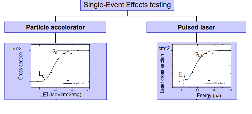
Figure 3: Comparison of pulsed laser and particle method cross section vs. LET curves
In the figure above σLS, E0. σs and L0 represent laser saturation cross section, laser SEE threshold energy, particle saturation cross section and particle SEE threshold energy respectively.
For the SDRAM test, the Device Under Test (DUT) was placed exactly underneath the camera system and the laser beam. Both the IR beam from the illuminator and the laser beam were focused on the sensitive volume. As the translation stage was by the laser beam moved, the device under test was scanned and the image of DUT was observed by the IR camera. A strip along the center part of the SDRAM contained most of the control logic and its feature were resolvable under the microscope as shown in figure 4.

Figure 4: The resolved comb-like structure at the center of the SDRAM which is observed in the picture, contained most of the control logic and caused most of the logic errors.
However, the memory array was located on either side of this strip down the center of the SDRAM and the resolution of the microscope (nearly 1 micron) was not high enough to resolve its features as depicted in figure 5.

Figure 5: The resolution of the microscope was not high enough to resolve the individual memory cells
The types of errors which were observed during these tests were
SEU (Single Effect Upset), where a state of a bit was reversed
Small logic errors, causing 20 upsets
Block errors, causing upto 20-4096 upsets
SEFI (Single Effect Functional Interrupt), which required a power cycle for recovery
The heavy ion testing was influenced by the TPA testing. The main goals of heavy ion testing was to identify the vulnerability to SEFI, inter-comparison between the error modes induced in laser testing and heavy ion testing and finally determination of cross section vs. LET curves for different error modes such as SEU, SEL and SEFI. One pre-determined strategy for the heavy ion testing was to mask parts of the logic circuit to separate the logic circuit errors from memory cell errors. However the laser testing proved that the control logic is also scattered in the memory array and therefore this masking strategy will not be effective.
Several heavy ions were used during the heavy ion testing including Ne, Ar, Kr and Xe beams but a SEFI error could only be observed once during a Kr heavy ion testing. The LET for this Kr ion beam was about 22 Mevcm2/mg and its symptoms of this error mode were very similar to that of laser pulse testing. It required a reboot of the system to be cleared and it is likely that this error mode happened only during a small part of the operation of SDRAM.
In conclusion, TPA laser testing can be used as a very effective tool to evaluate the SEE response of a system prior to heavy ion testing. Inducing and observing the occurrence of different error modes using the laser pulse testing method elucidates what to expect during heavy ion testing and preparation can be made as far as test methods, hardware, software and analysis is concerned before a trip to heavy ion testing facility.
Allied Scientific Pro has designed a SEE testing pulsed laser based SPA system which has the potential to be upgraded to a TPA system. A video of the system can be found in the following link:
https://photos.app.goo.gl /qRxrgvGaDejq416V8
Reference: R.Ladbury et.al, TPA laser and Heavy ion SEE testing: Complementary techniques for SDRAM Single Event Evaluation, IEEE transaction on nuclear science (TNS), December 2009.